PRuggiero
Mechanical
- Oct 8, 2007
- 64
I'm making my head hurt because I think i'm making something harder than it needs to be.
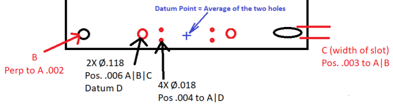
I have a Circuit board that interfaces with a heatsink through two pins (part of the heatsink) with a hole (Datum B) and slot (Datum C defined by the width). There is a pattern of holes (two Ø.118 and 4 smaller ones) that are for a connector. This is all shown in picture 1.
Link
It is more important for the connector holes (really the Ø.118 ones) to be oriented to the A|B|C datum structure than it is to be located.
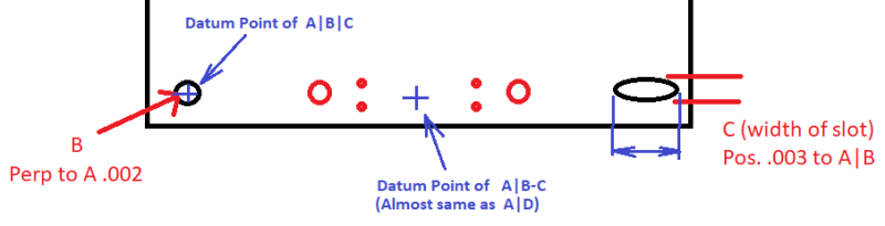
Picture 2 seems to make the most sense to me with respect to accomplishing my goals.
Link
Picture 3 is what i am more used to seeing, what I don't understand is how this controls the orientation relationship between B-C and D-E since Datum E is only positioned relative to A|D.
Link
Thoughts/Feelings?
Thanks,
Pete
I have a Circuit board that interfaces with a heatsink through two pins (part of the heatsink) with a hole (Datum B) and slot (Datum C defined by the width). There is a pattern of holes (two Ø.118 and 4 smaller ones) that are for a connector. This is all shown in picture 1.
Link
It is more important for the connector holes (really the Ø.118 ones) to be oriented to the A|B|C datum structure than it is to be located.
Picture 2 seems to make the most sense to me with respect to accomplishing my goals.
Link
Picture 3 is what i am more used to seeing, what I don't understand is how this controls the orientation relationship between B-C and D-E since Datum E is only positioned relative to A|D.
Link
Thoughts/Feelings?
Thanks,
Pete